Last time, we learned the basics of transistors. Now, it’s time to learn about logic gates. Logic gates can be built using transistors and are the fundamental building blocks of any complex digital circuit. In this post, we will cover how logic gates work in principle. In a future post, we will then see how logic gates can be built using transistors.
Let’s get started!
Logic Operations and Truth Tables
As the name suggests, logic gates perform so-called logic operations. A logical operation takes some inputs and combines them in a specific way to produce an output. Each input can be either “true” or “false” (or “1”, or “0”). The same holds for the output. For example, the logical “AND” operation has two inputs, let’s call them A and B, and one output, that we name Z. The output Z will only be “true” when both A and B are “true”; hence “and”.
The behavior of any logical operation can be represented using a special table, called the truth table. The truth table shows for all possible input combinations the corresponding output values, thereby fully characterizing the function of the particular logic operation. For example, the truth table of the AND operation looks like this:
| A | B | Z = A and B |
|---|---|---|
| 0 | 0 | 0 |
| 0 | 1 | 0 |
| 1 | 0 | 0 |
| 1 | 1 | 1 |
As you can see in the last row, the output Z is only “on” (1) when both inputs, A and B, are “on”; otherwise, the output stays “off” (0). Let’s look at the truth table of another logic operation, the OR:
| A | B | Z = A or B |
|---|---|---|
| 0 | 0 | 0 |
| 0 | 1 | 1 |
| 1 | 0 | 1 |
| 1 | 1 | 1 |
Can you see the difference of the OR compared to the AND operation? The OR operation produces a “1” at its output when at least one input is set to “1”. This behavior is also what its name suggests: A or B (and that also includes the case when both A and B are 1). Another interesting logic operation is the NOT operation:
| A | Z = not A |
|---|---|
| 0 | 1 |
| 1 | 0 |
The NOT operation only has one input and one output. Again, as the name suggests, the NOT operation simply produces the inverse (or the negation) of its input.
Now, buckle up! Your mind is about to be blown away: With only the three logic operations we presented you above, namely the AND, OR, and the NOT operations, it is possible to construct ANY digital circuit, even the processor you are using to read this blog post1!
Next, we will learn how this is done in practice.
Basic Logic Gates
Logic operations are implemented in hardware using logic gates. Just like a logic operation, a logic gate has inputs and output(s). For example, this is the logic gate for the AND operation, or short, AND gate:
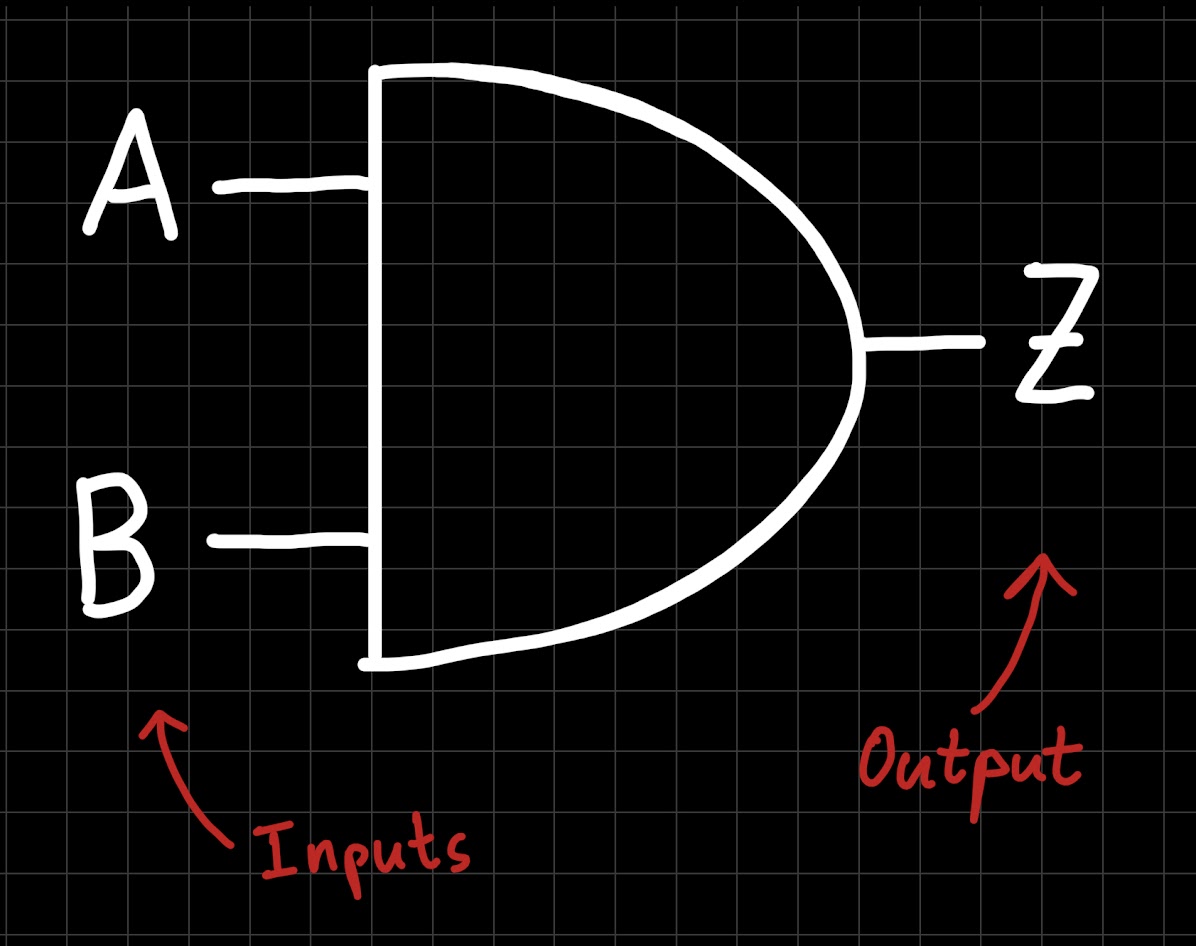
To be fair, this is not how the AND gate looks on the final chip, in reality, but this is how we represent an AND gate when drawing logic circuit diagrams2. As we mentioned initially, we will see in one of the next post how logic gates are really implemented in hardware. For now, it is sufficient to view logic gates as black boxes that take inputs, perform logical operations, such as AND, on the inputs and produce an output.
In the following, we show you some other gates that implement the logic operations we introduced above.
This is the symbol of the OR gate:
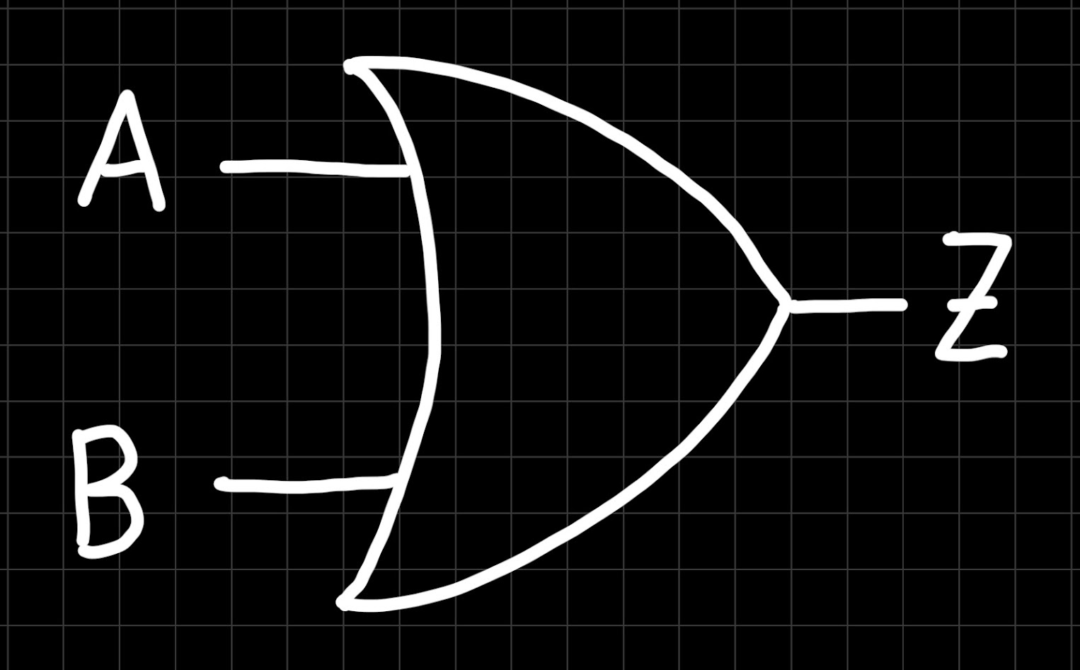
And this is the NOT gate:
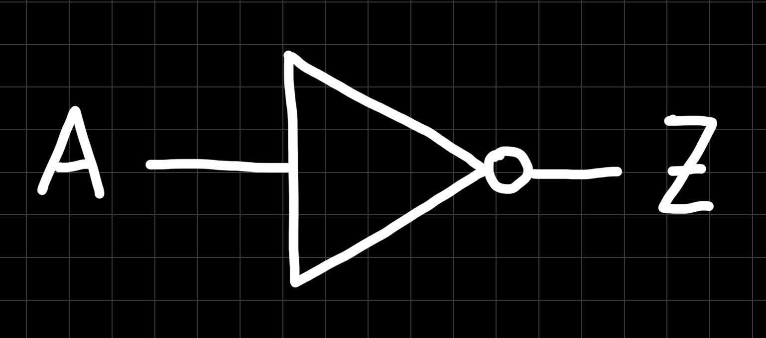
These were the most basic gates. Next, let’s have a look at some more complex gates!
Complex Logic Gates and Circuits
As the output of a logic gate is also a binary value (0 or 1), nobody hinders us to connect multiple logic gates together to perform more complex operations! For instance, can you figure out the truth table of the following circuit:
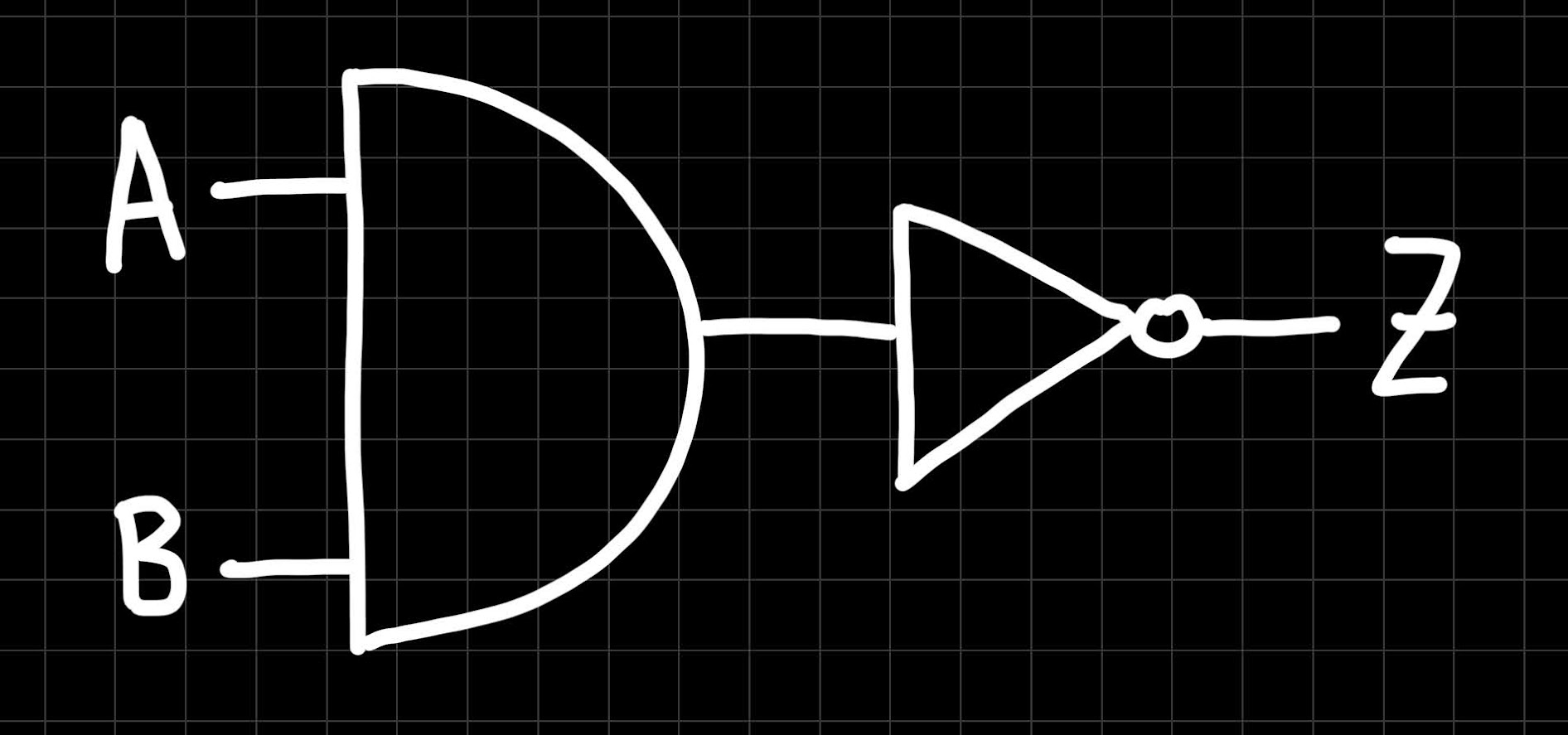
Here is the solution:
| A | B | Z |
|---|---|---|
| 0 | 0 | 1 |
| 0 | 1 | 1 |
| 1 | 0 | 1 |
| 1 | 1 | 0 |
If you got it right, pat yourself on your shoulder! If not, that’s totally fine, we will explain to you now how it works: this “combined gate” has two inputs, A and B. We have to look at all possible input value combinations (there are four of them). These inputs first go into the AND gate, and its truth table we already know:
| A | B | “A and B” |
|---|---|---|
| 0 | 0 | 0 |
| 0 | 1 | 0 |
| 1 | 0 | 0 |
| 1 | 1 | 1 |
Now comes the crucial part. The output of the AND gate is at the same time the input of the NOT gate! Therefore, to determine the output of the NOT gate, and hence the overall output, Z, we consult the truth table of the NOT gate and use the values in the “A and B” column as its input:
| A | B | “A and B” | Z |
|---|---|---|---|
| 0 | 0 | 0 | 1 |
| 0 | 1 | 0 | 1 |
| 1 | 0 | 0 | 1 |
| 1 | 1 | 1 | 0 |
Remember, when the input is 0, the NOT produces a 1, and vice versa. There we go, we constructed our first truth table!
This combination of an AND gate followed by a NOT gate is quite common in digital circuits, therefore they have been merged into one single gate, called the NAND gate. Its symbol looks like this:
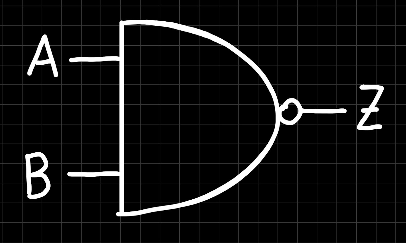
Basically, we just took the circle from the NOT gate and stuck it at the output of the AND gate to indicate that the output is negated. We can do the same with any other logic gate, such as the OR gate:
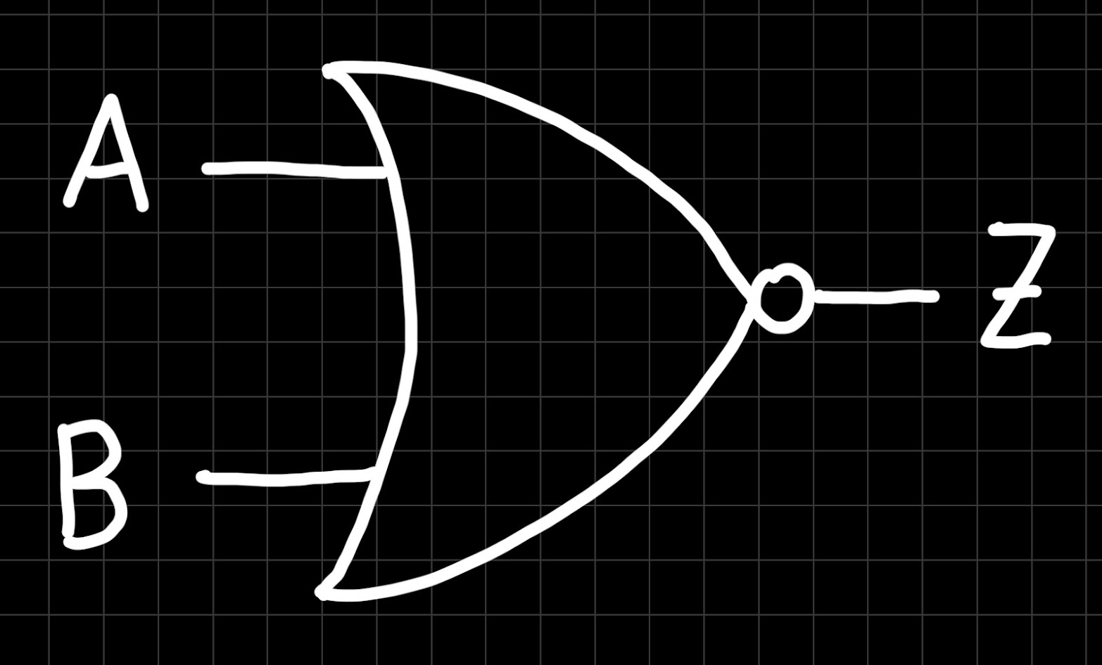
This gate is similarly called NOR gate. As an exercise, try to write down the truth table of a NOR gate!
Let’s look at some more examples. Again, first, try to figure out the truth table of the following circuit by yourself:
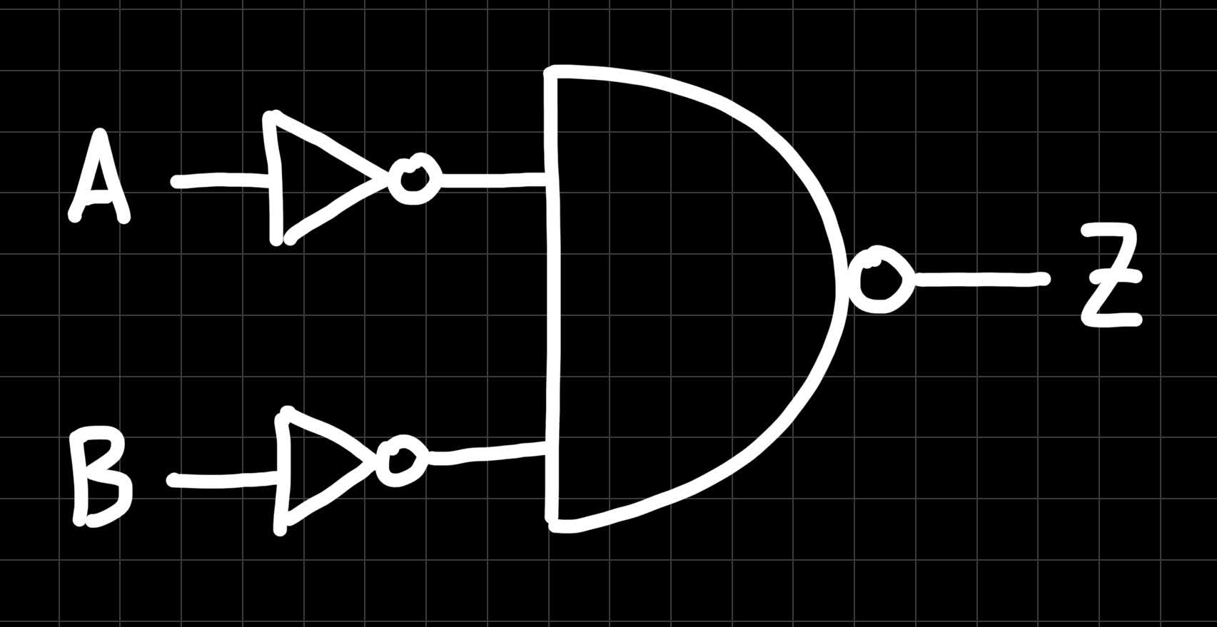
Got it? Here is what you should have gotten:
| A | B | Z |
|---|---|---|
| 0 | 0 | 0 |
| 0 | 1 | 1 |
| 1 | 0 | 1 |
| 1 | 1 | 1 |
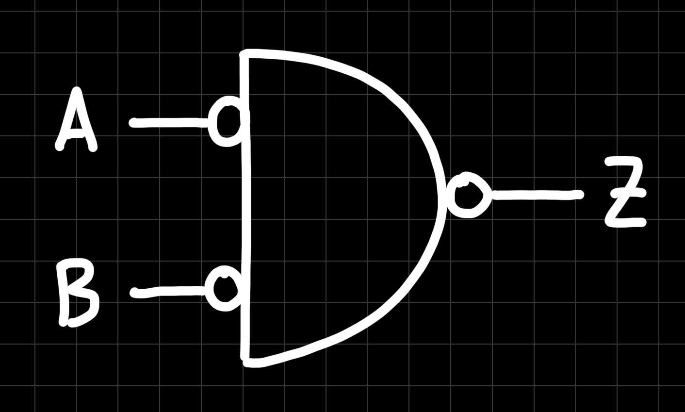
Do you remember this truth table? Right, this is an OR gate! This means, that we can construct an OR gate from two NOT gates and one NAND gate. By the way: When some inputs of a gate are inverted, like in the example above, we don’t have to draw the full NOT gates. Similar to how we draw a small circle at the output of the NAND gate, we can also draw circles at inputs to indicate that these are inverted. For instance, here is the simplified version of the example above:
Here’s another more complex circuit. Try to work out its truth table:
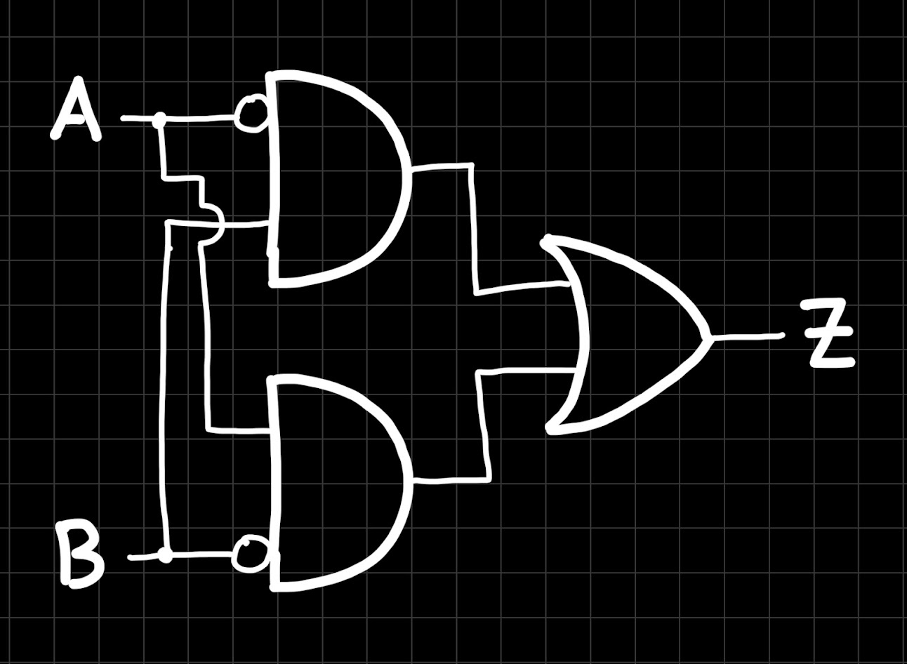
Hint: When two wires cross without touching each other in a circuit diagram, we draw a little arc. In the circuit above, you can see an example at the upper AND gate, where the wire A crosses wire B without touching.
This is the truth table of the circuit:
| A | B | Z |
|---|---|---|
| 0 | 0 | 0 |
| 0 | 1 | 1 |
| 1 | 0 | 1 |
| 1 | 1 | 0 |
Do you notice a pattern in this truth table? The output is only “on” when exactly one input is turned on. And in fact, this behavior turns out to be so important in digital circuits, that there is even a dedicated logic gate for it: the XOR gate (XOR stands for “exclusive OR”). The XOR gate has the following symbol:
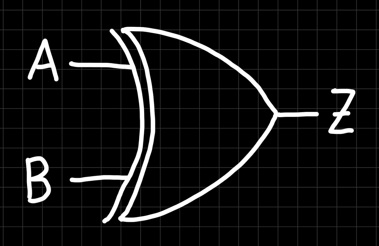
And, with this, we have covered most of the basic logic gates! For those of you who like a little challenge, we have prepared the following circuit:

Can you figure out its truth table? We have already prepared it for you:
| A | B | C | Z |
|---|---|---|---|
| 0 | 0 | 0 | ? |
| 0 | 0 | 1 | ? |
| 0 | 1 | 0 | ? |
| 0 | 1 | 1 | ? |
| 1 | 0 | 0 | ? |
| 1 | 0 | 1 | ? |
| 1 | 1 | 0 | ? |
| 1 | 1 | 1 | ? |
We will present you the solution in our next post, so don’t miss that!
Wrap-up
To conclude this post, let’s summarize what we’ve learned:
- Logic gates perform logical operations
- The behaviour of a logic gate can be described using a truth table
- We have learned the following basic logic gates:
- AND
- OR
- NOT
- NAND
- NOR
- XOR
Stay tuned for our next post, and make sure to follow us on Twitter, so you don’t miss it when it comes out. See ya!
-
For the people that are already screaming: Yes, you need a bit more than just logic operations to build a processor, but for the digital part of the chip, the statement is true. ↩
-
There are also other ways to draw logic gate symbols. The logic gates we showed you here, are part of the ANSI standard. Other standards are IEC, or DIN. In our blog series, we will continue to use the ANSI gates. ↩