We from Bits&Volts hope that, despite the current circumstances, you had a nice transition into 🎆2022! Let’s hope that things get better this year. Whatever comes, we will keep writing our blog posts, so you always have something to learn!
Now, let’s start this year with the second part of our Introduction to Logic Gates series. Last time, we have seen what kind of logic gates there are. This time we will learn how these gates can be built using transistors. But before we dive in, let us first show the solution to last post’s challenge. In case you don’t fully remember (to be fair, it’s been some time…), this was the circuit for which we asked you to create its truth table:

And here is the solution, its truth table (we also added labels for intermediate values):
| A | B | C | u | v | w | Z |
|---|---|---|---|---|---|---|
| 0 | 0 | 0 | 0 | 0 | 1 | 1 |
| 0 | 0 | 1 | 0 | 1 | 1 | 0 |
| 0 | 1 | 0 | 0 | 0 | 1 | 1 |
| 0 | 1 | 1 | 0 | 1 | 1 | 0 |
| 1 | 0 | 0 | 0 | 0 | 1 | 1 |
| 1 | 0 | 1 | 0 | 1 | 1 | 0 |
| 1 | 1 | 0 | 1 | 1 | 0 | 1 |
| 1 | 1 | 1 | 1 | 1 | 0 | 1 |
Did you get it right? If not, don’t worry, just try again. And in case you are completely stuck, feel free to use our comment function below, and we can help you out!
Let’s continue with this post!
CMOS
Before we start, let’s get some terminology out of the way. As a reminder, in our post about transistors, we have seen how the schematic symbols of NMOS and PMOS transistors look like:
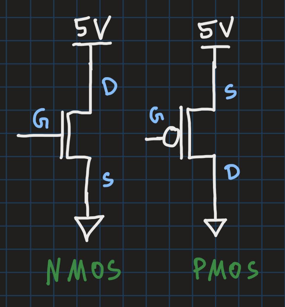
As you can see in the picture, the upper parts are each connected to something called “5V”. What does that mean? “V” stands for Volts, and as you probably guessed, it is the unit for voltage. In digital circuits, voltages are used to represent binary (or logic) 1s and 0s. Two voltages are sufficient, and usually, the higher of the two represents a binary 1, and the lower a binary 0. Common voltages for binary 1s are 5V or 3.3V. In our example above, the drain (of the NMOS) is connected to 5 Volts. So this circuit uses 5V to represent a binary 1. What about the triangle thingies at the bottom? This is what we call ground. It is the reference potential1 and can be viewed effectively as 0V. You probably guessed it: 0V represents a binary 0.
An NMOS transistor turns on (i.e. opens its channel) when some voltage larger than its threshold voltage is applied to its gate. The threshold voltage is different from transistor to transistor. For the NMOS transistors used in this post, we assume that 5 Volts are well above their threshold voltage, and therefore, they turn on. The PMOS transistors behave opposite to NMOS transistors: they turn on when the gate voltage is 0V, and they turn off when 5V are applied to their gate. From now on, we will use the binary values for the gate voltages: 1 means that 5V are applied to the gate, and 0 means 0V.
Most modern chips make use of a technology called CMOS. CMOS stands for Complementary Metal-oxide semiconductor. The “MOS” part might be already familiar to you: this refers to the MOSFETs, we already learned about. The “complementary” means, that in CMOS circuits, always pairs of NMOS and PMOS transistors are used. The reasons why pairs of transistors are used are beyond the scope of this post, but just keep that fact in mind. In the following, we will see plenty of examples.
Inverter
The most basic CMOS circuit is the CMOS inverter and consists of two transistors. One PMOS and one NMOS:
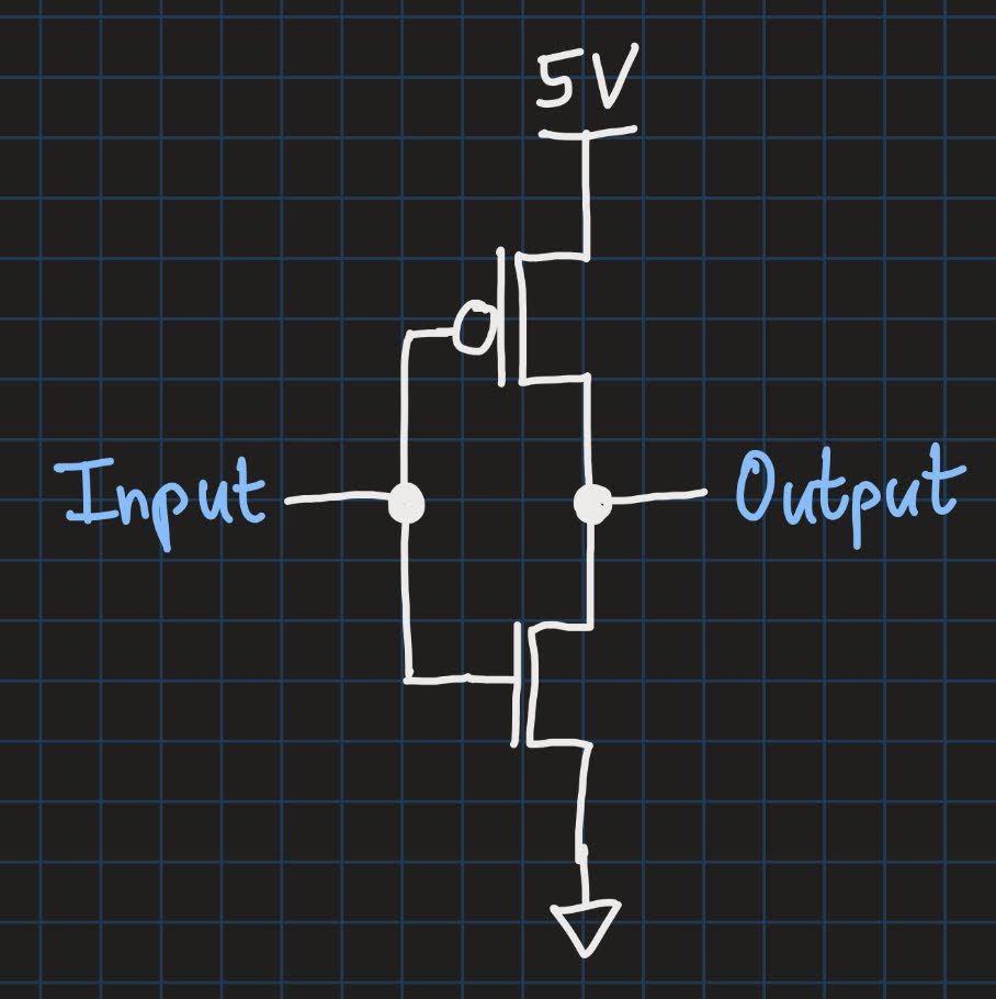
The input on the left goes into the gates of both transistors. The output on the right is connected to the middle section between the two transistors. You may remember from our last post that an inverter just flips a 1 to a 0, and vice versa. Let’s try to see this in the circuit.
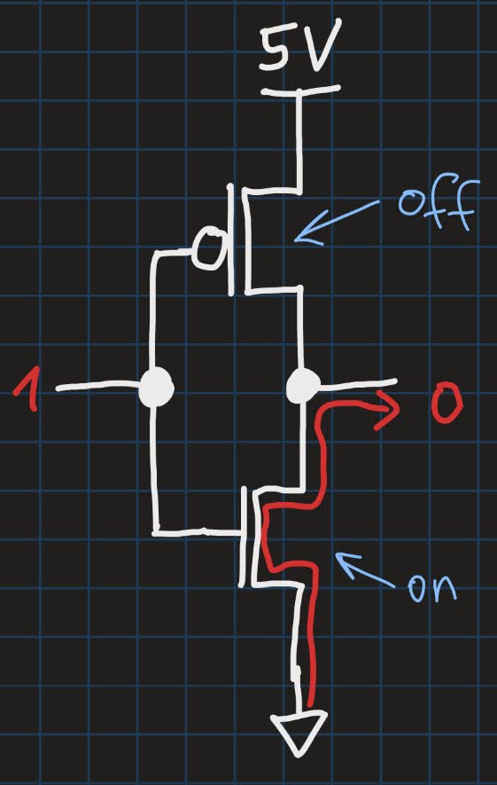
First, we look at when the input is a logic 1. Recall that a logic 1 is represented in the hardware as a voltage, e.g. 5V, and a logic 0 is usually 0V. Both transistors will see a 1 (5V) at their gates. The NMOS will consequently open the channel, thus effectively connecting the output to ground (or 0V). So, the output will be seen as a logic 0 - just like you would expect from an inverter! But what about the upper PMOS transistor? Well, when a PMOS sees logic 1 at its gate, it will “shut off”, i.e. the channel is closed, meaning no current can flow from the 5V terminal to the output. Therefore, the output is only influenced by the NMOS, which “pulls down” the output to 0:
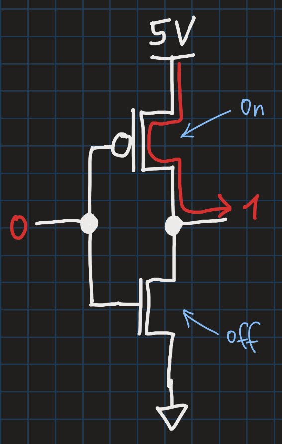
In the other case, namely, when the input is a logic 0, things just work the opposite way. Now, the NMOS will switch off, thus cutting off the output from ground. The PMOS will open its channel, and a current can flow from the upper 5V terminal, through the PMOS, all the way to the output. We say that the PMOS “pulls up” the output to 5V. An observer at the output pin will see 5V, and thus a logic 1 - just as you would expect from an inverter.
We hope this wasn’t too confusing. Let’s look at some more logic gates.
NAND gate
The NAND gate looks a bit more complicated than the inverter. It has four transistors: 2 PMOS and 2 NMOS. In the following picture, we also included the truth table of a NAND gate, in case you don’t remember it exactly:
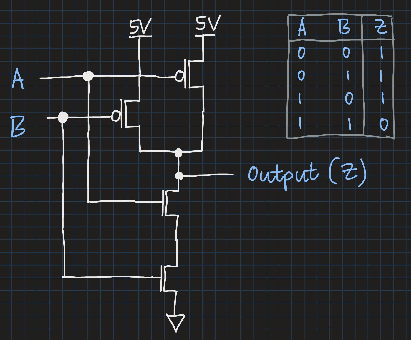
First, we notice that each input goes to one PMOS and one NMOS at the same time. If we look closely, we can see a slight difference in the arrangement of the PMOS and NMOS transistors. The two NMOS transistors are connected in series. This means that there is only one path from ground to the output. On the other hand, the two PMOS transistors are connected in parallel: there are multiple ways (two in this case) in which current can travel from the 5V terminal to the output. Ok, so what’s the deal with that?
Since the NMOS are in series, both need to be turned on for a current to flow between ground and output (in other words, to pull down the output to 0). For the PMOS, to pull up the output to 1, it is sufficient when at least one PMOS is turned on.
When both inputs A and B are a logic 1, both NMOS transistors will open, allowing a current to flow between ground and the output. At the same time, both PMOS transistors will switch off. The output will see a logic 0. This exactly matches with the last row of the NAND gate’s truth table.
In all other cases, i.e. when at least one of the inputs is a logic 0, at least one NMOS will switch off, thereby breaking the series connection, and no more current flow between ground and the output will be allowed. On the other hand, at least one PMOS will open its channel, and a current can flow between the 5V terminal and the output - the output becomes a logic 1. Again, this matches precisely with the first three rows of the truth table!
To make it more clear for you, the following picture shows the resulting paths for each input combination:

NOR gate
The NOR gate looks similar to the NAND gate. But notice that now, the PMOS transistors are connected in series, while the NMOS are in parallel:
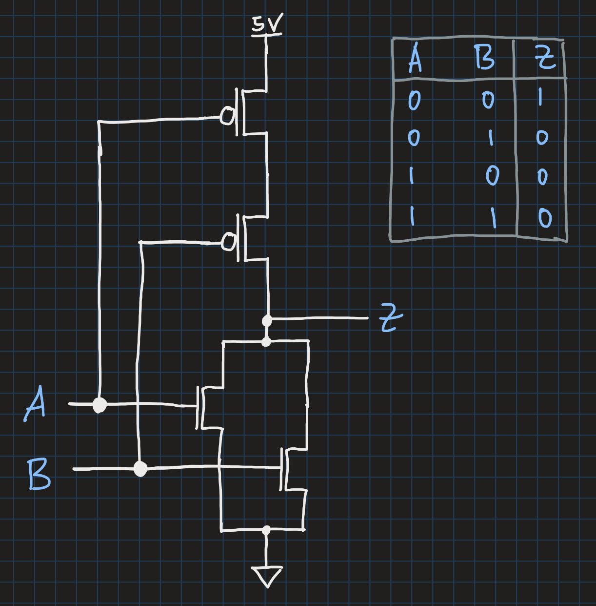
Only in the case when both inputs are a logic 0, both PMOS transistors will open, and a current can flow from 5V to the output. At the same time, both NMOS will cut off the connection to ground. Therefore, the output is a logic 1.
In all other cases, when at least one input is 1, at least one PMOS will break the path from 5V to the output, and at least one NMOS will open the path from ground to the output. Therefore, the output is a logic 0.
AND/OR gate
Next, let us look at the how the AND gate looks:
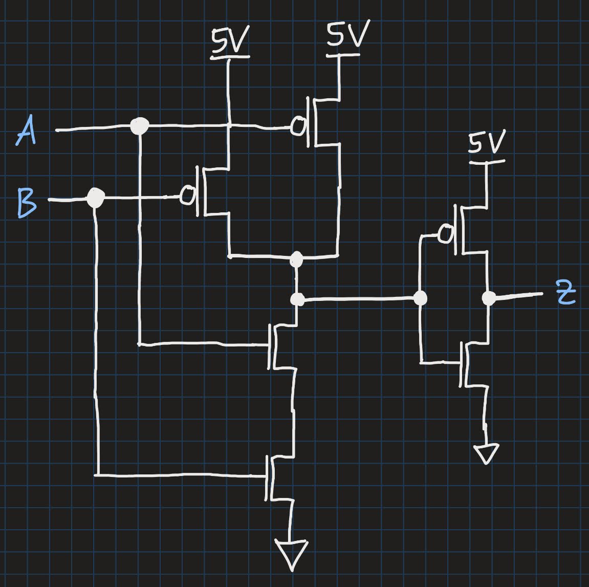
Do some parts of the circuit look familiar to you? Right! There is a NAND gate, followed by an inverter! If you remember from our last post, a NAND gate itself is just an AND gate, followed by an inverter. So, when a NAND gate is then again followed by an inverter, we again get an AND gate. But why is it done like that?
It has to do with how NMOS and PMOS fundamentally work. However, explaining the details here is out of the scope of this post. Just note, that in all CMOS circuits, the PMOS transistors are always in the upper part, namely at the 5V section, while the NMOS transistors are in the lower part, i.e. near ground. The PMOS section is often referred to as a pull-up network because when there is a path from the 5V terminal to the output, the output always gets pulled up to 5V as well, as we have seen in the previous examples. Similarly, the NMOS section is called pull-down network, because it pulls down the output to 0V.
Forcing all PMOS transistors into the pull-up network and all NMOS transistors into the pull-down network, respectively, might sound like a limitation. However, due to the semiconductor physics of these two types of MOSFETs, it is indeed the most optimal way to design CMOS circuits.
And that’s why an AND gate is constructed using a NAND + Inverter. An AND gate, therefore, consists of six transistors. If you still don’t believe us: try designing a CMOS AND gate with less than six transistors, and where all PMOS transistors are in the pull-up network, and all NMOS transistors are in the pull-down network. (hint: you will successfully fail).
What about the OR gate? We leave that task to the reader, it’s not that difficult if you understood how the AND gate is made! (you can also find the solution in the next section ;)
Complex circuit
Let’s put it all together - quite literally. We will show you how the transistor schematic of the circuit from last post’s challenge looks like. Here is the circuit again:

A little warning: don’t be scared, this is the transistor implementation of the same circuit:
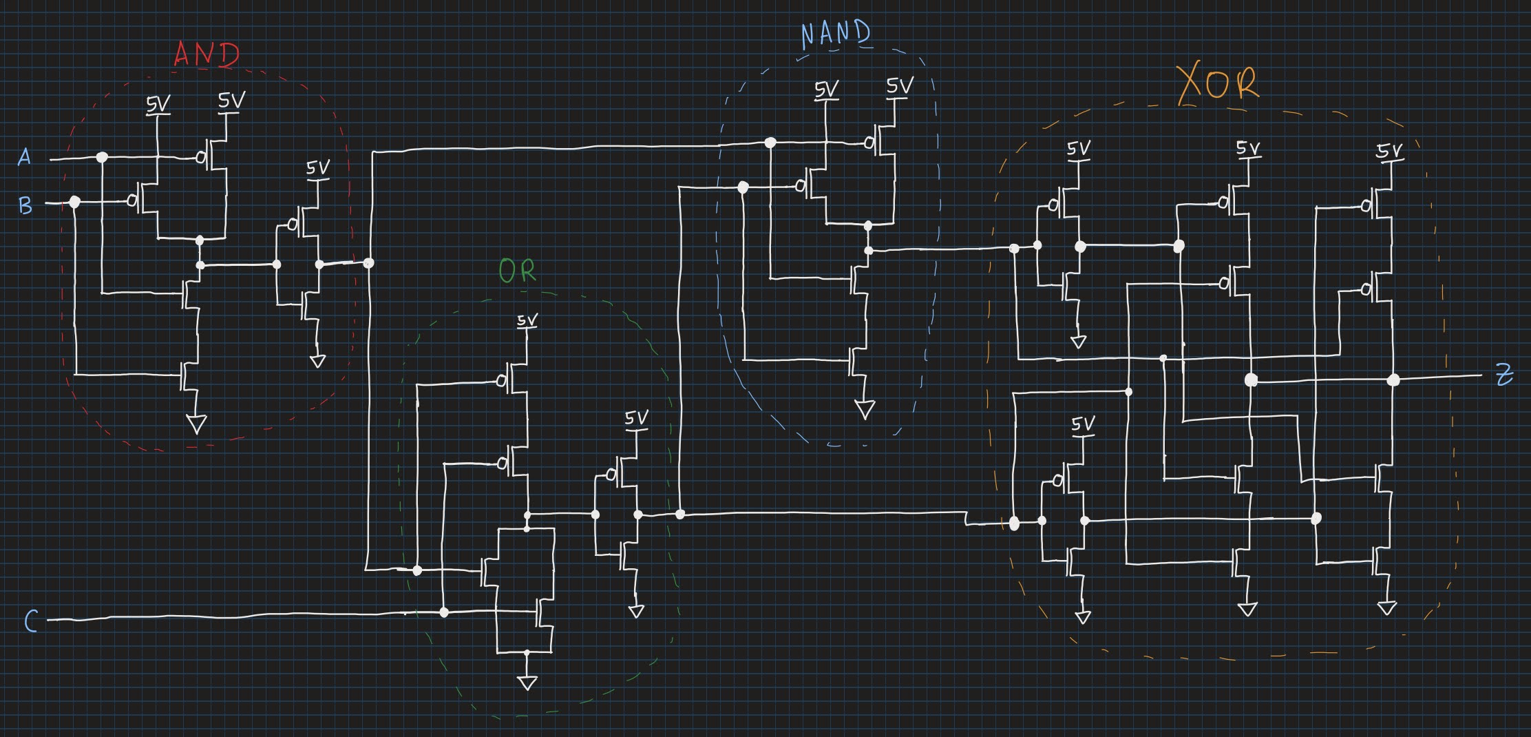
To make it easier for you, we have circled the logic gates in different colors. We can recognize the CMOS transistors of the AND, OR, and NAND gates. The CMOS XOR we didn’t show you earlier, but from the circuit, you can see that it looks much more complex than the other gates. Overall, this circuit made up of just four logic gates already consumes 28 individual transistors! Drawing this by hand is still somewhat manageable. But think of a big processor: those beasts consist of millions of logic gates (not transistors). And since each gate is made up of multiple transistors itself, you can imagine, that designing an entire CPU by hand is straight up infeasible nowadays! That’s why we have to use the help of Electronic Design Automation (EDA), i.e. software to automate the design of digital circuits, when we build such complex chips. These tools will do the mapping from logic gates to transistors fully automatic! If you are interested, we can do a post about EDA, what tools there are and how they work; let us know in the comments (we might do it anyway ;)
Physical Layout
One final note. Remember when we said in our last post, that the symbols we use for drawing logic gates were not how the actual gate would look in hardware? Well, even the transistor diagrams we showed you in this post don’t depict how the real hardware looks, but they are already pretty close! In case you are wondering, here is how a NAND looks on the final chip:

“This looks nothing like the schematics you showed us in this post!?”, you may ask yourself. That is a valid question! Let us explain what’s going on here. If you have read our very first post in the Digital Design series, you may remember that there are a lot of steps involved when making a microchip. One of these steps is physical design, which comes shortly before manufacturing the chip. In this step, the circuit design consisting of thousands or millions of logic gates is transformed into a so-called layout. The layout describes how the individual transistors and the wires connecting them should be laid out on the final chip2. The layout is the final blueprint for the manufacturing. We have to admit that the picture above does not show a real photo3 of a NAND gate. However, the structures are in fact how they would look on the final chip, though without any colors.
Physical design in itself is so complex, that there are engineers who just work on optimizing the layout of a chip. Nowadays, with the advent of sophisticated EDA tools, this task is being automated more and more. However, a lot of research and manual handwork still goes into optimizing the physical layout of individual gates, to make them even smaller and faster. That’s why the NAND gate layout above doesn’t look at all like the schematic at first glance. However, the layout was simply optimized in such a way to consume the least amount of area (chip area = more money you have to pay the foundry), but the fundamental transistors and their connections are still there, so the layout it still implementing the NAND gate’s schematic.
Summary
If this post was too much information to take in, don’t worry. In this blog series, we will focus on higher-level digital design, and the lowest we will ever go to is the level of basic logic gates. With this post, we just wanted to show you how the gates are implemented in hardware, so you can at least say “I have seen how logic gates are implemented on a chip”, and that already would make us happy :)
As we now have reached the end of this post, let us quickly summarize the key ideas we have learned:
- CMOS stands for “Complementary Metal-Oxide Semiconductor”
- In CMOS there are always PMOS / NMOS pairs
- The PMOS transistors are part of the pull-up network, and the NMOS transistors belong to the pull-down network
- The CMOS inverter consists of one PMOS and one NMOS transistor
- The CMOS NAND and NOR gates consist of two PMOS and two NMOS transistors
- We have learned about series and parallel connections
- An AND gate is built using a NAND gate followed by an inverter
- Similar for the OR gate: NOR followed by an inverter
- We have learned what a physical layout is, and, as an example, have seen how a NAND gate looks in the layout
We hope you liked this post, and, as always, thanks for reading! Follow us on Twitter to don’t miss any of our future posts!
-
There are no absolute voltages. A voltage is always a potential difference. Therefore, every electric circuit needs some kind of reference potential, a baseline, and all other voltages are relative to this reference. We might do a future post on the basics of electronics where we explain in depth what voltage, current, etc are. ↩
-
Additionally, physical aspects like size and power consumption are considered. ↩
-
Taking a photo of nm-sized gates using a conventional camera is not possible, as visible light has a much bigger wavelength compared to modern gates sizes! However, we can use a scanning electron microscope instead. Check out this video if you are interested. ↩